You can also be interested in these:
- NVIDIA GeForce GT 720 review
- NVIDIA GeForce GTX 1050 Ti Max-Q review
- NVIDIA Quadro FX 3800 review
- Nvidia Geforce GTX 560 Full Review
The end of 2022 is seeing accelerated development in the PC components market, with new CPUs from AMD and Intel in a battle to the top, and now Nvidia is making its move by presenting its flagship model, none other than the Nvidia RTX 4090, debuting the 4 nm Ada Lovelace architecture.
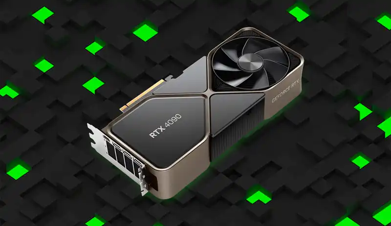
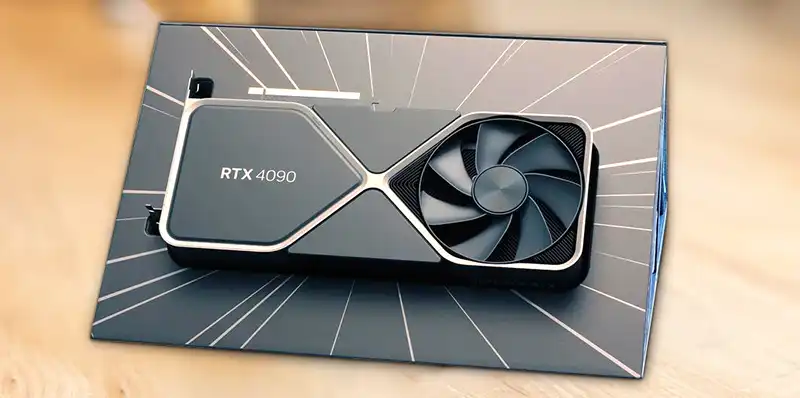
Enormous in every sense, it is the most monstrous Nvidia model we have seen, with 60 mm thickness and an impressive unibody aluminum heatsink that maintains the Ampere aesthetic. It is not surprising with a 23-phase PCB to power the 450W AD102 chipset, 128 SMs, and 24 GB of GDDR6X VRAM exceeding 2.5 GHz clock speed. How much more powerful is it compared to the 3090 Ti? Is it as much as previous benchmarks say? We will see below!
Design and heatsinks are the same as Ampere models
The heatsink design could be said to serve more aesthetic requirements than thermal performance. The Nvidia GeForce RTX 4090 has followed this same design, but its size factor has grown considerably. It has dimensions of 336 mm long, 140 mm wide, and 60 mm thick, occupying 3 slots on the motherboard. The same as the RTX 3090 Ti model.
After all, it makes sense to adopt virtually the same heatsink as the flagship of the previous generation, as both have specified 450W TGP. However, there are slight modifications that we can point out, such as the slightly inward-curved corner design to refine the lines of the assembly. We still have a white LED lighting zone in the “GEFORCE RTX” logo and in the triangle leading to the upper fan.
We position ourselves on the bottom face of the Nvidia RTX 4090 to see a wide 115 mm diameter axial fan in push mode, taking better advantage of the heatsink area that is just above the PCB and chipset. This is responsible for introducing air inward, contained on a unibody chassis with an “hourglass” design with thick aluminum plates that interweave the fully visible heatsink. No screw can be seen as it is under carefully placed covers, making it quite difficult to disassemble.
Under the fan, we have an aluminum block with fins placed longitudinally directing the air towards the air outlet through the rear area. A second block located in the center has diagonal fins that combine with the last block placed in the second zone of the sand clock.
The concept of axial flow is adopted as this area remains open below, so that the upper fan in pull mode can pass the air and cool this entire area as effectively as possible. Going into a bit more detail, one can see the internal cooling block built in copper, which distributes the heat throughout the available volume through 6 heat pipes.
We move to the top where we have the entire area covered with plastic covers except for the fan. These elements act as a backplate although the effectiveness of the heat sink may be reduced a bit, taking advantage of the area to stamp the model of the card in question. Finally, at the front edge, we have a small cover that hides the anchoring system for external card support provided with two holes.
The 2-fan system will be managed automatically by the GPU, with zero RPM mode when it is under low load and below a certain temperature threshold. Obviously, they can be controlled individually from some software such as Afterburner or similar in case of overclocking.
Ports and connections
The port panel of the Nvidia RTX 4090 is another element that remains unchanged from the previous generation with a total of 4 ports distributed in 3 DisplayPort 1.4a ports and 1 HDMI 2.1 port.
Above them is a huge opening extended towards the left edge where the air is evacuated. We remind you once again that the HDMI 2.1 port supports maximum resolutions of 8K @120 FPS and 60 FPS compressed and up to 4K @144 Hz uncompressed, with more bandwidth than the operational version of DisplayPort.
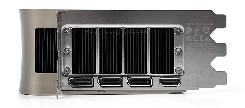
The most relevant information comes in terms of its connection and power interface. First of all, this card does not have SLI or NVLink connection, so the ability to operate with parallel GPU is finally abandoned as it has little practical application today. It will continue to use the PCIe 4.0 or Gen4 interface with 16 active lanes, which is more than enough for the capacity of current monitors and Resizable Bar technology, leaving Gen5 for future generations.
Regarding the power system, we only have a unified 16-pin PCIe header of the latest generation, which is the path followed by Nvidia to minimize the number of headers on the PCB and wiring in the PSU. Being a very recent interface, a 16-pin to 4 8-pin PCI header converter dongle is included. Of these, we are only obliged to use 3, as the 4th will only be necessary if we plan to overclock the graphics card. The 16-pin connection is designed to support the 450W TGP specified by the card, we hope that the power supplies are up to the task with good connectors and thick cables.
Ada Lovelace Architecture: Hardware and Software innovations
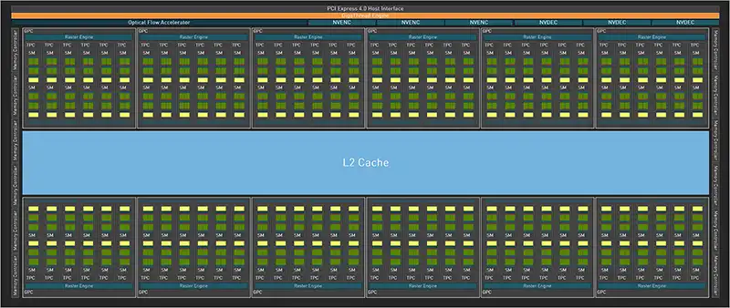
Nvidia introduces its new Ada Lovelace architecture, which is based on a 4 nm manufacturing process by TSMC customized by Nvidia. Smaller lithography means more transistors per unit area, and this Nvidia RTX 4090 has a chipset of 608.5 mm2 with no less than 76.3 billion transistors compared to the 28.3 billion of the RTX 3090 Ti, more than double. This allows for improved IPC and energy efficiency, in fact the consumption of this unit will be 450W, the same as specified for the 3090 Ti. The reference model has 22 power phases.
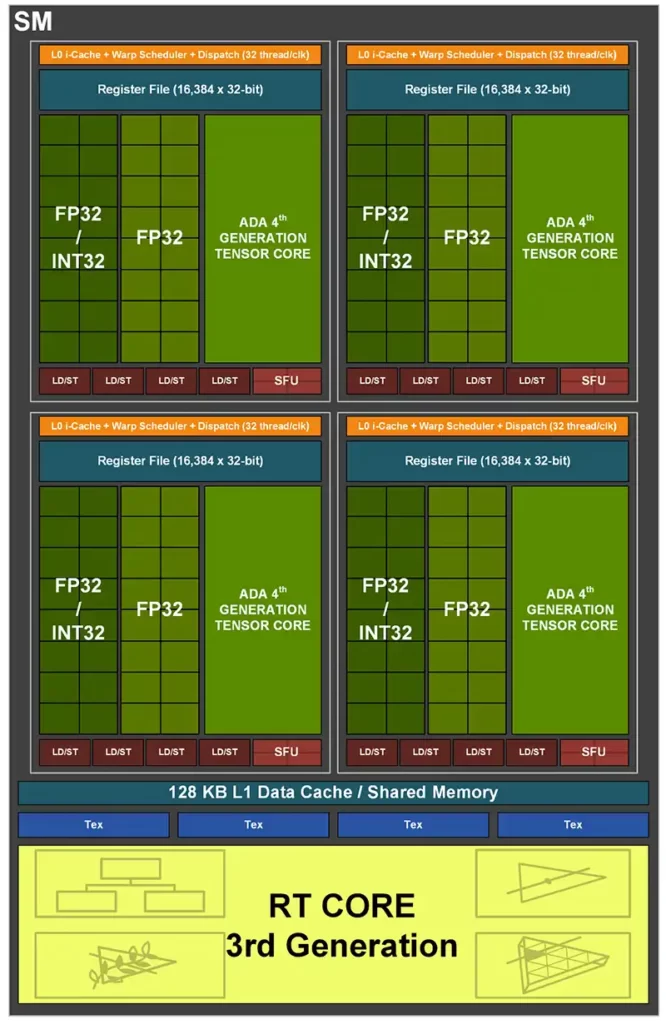
Nvidia GPUs still have integrated Streaming Multiprocessors as their processing unit, which in turn are divided into 1 RT (Ray Tracing) core, 4 Tensor cores and 128 CUDA (Compute Unified Device Architecture) cores. Together they offer a boost clock frequency of 2520 MHz in the reference 4090 version compared to the 1860 MHz achieved by the 3080 Ti. Not only AMD, but also Nvidia joins the 2.5 GHz club and rising, will we see RTX 4060 with over 3 GHz? The card generates a total of 512 TMUs and 176 ROPs compared to the 336 and 112 respectively of the RTX 3090 Ti.
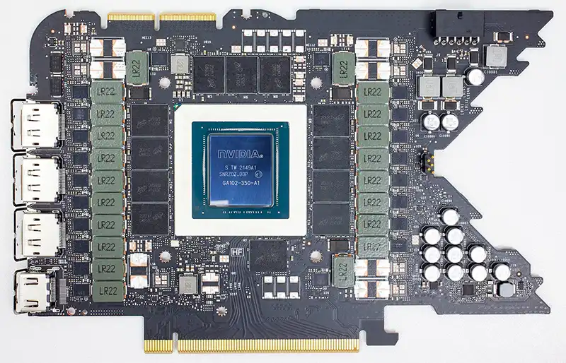
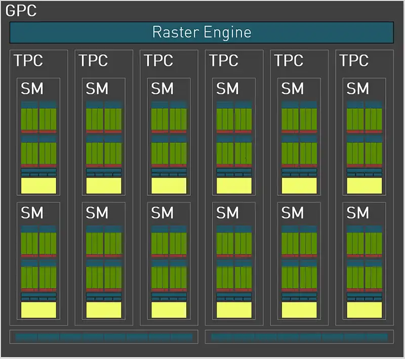
The SMTs are in turn within a high-level hardware unit called the GPC, which in this case is 11. This unit includes a dedicated rasterizing engine, two rasterizing operation partitions (ROPs), each with 8 ROPs and 6 TPCs with 2 SMs inside. This creates the complete AD102 chipset and the rest of the variants that will bring the RTX 40 models to life, with more or less GPCs inside.
With each generation, there are comprehensive updates to the internal cores. For example, the 16384 CUDA Cores that make up the AD102 chipset of the 4090 are capable of reaching 83 Shader-TFLOPS, more than double that of the Ampere architecture (40 TFLOPS). This improvement comes largely thanks to the Shader Execution Reordering (SER) technology, which is capable of reprogramming work and instruction queues on the fly, doubling its effectiveness.
The Tensor Cores become 4th generation and are counted as 512 units, whose function is to perform matrix operations, multiply, and accumulate mathematical operations for AI and HPC. They are the engine of the neural networks used in DLSS, and they accept a new FP8 format that was introduced in the Nvidia Hopper architecture. Compared to FP16, FP8 reduces data storage requirements by half, thus doubling AI capacity. This way its processing capacity is raised to 1.3 PetaFLOPS, surpassing the TeraFLOPS barrier comfortably.
The third component within the SM is the RT cores that are dedicated to processing the ray triangle to generate the light rays that fall on objects. There are a total of 128 3rd generation RT Cores in the Nvidia RTX 4090 chipset, which double the performance compared to the 2nd generation of Ampere, reaching 191 RT-TFLOPS. To achieve this, it introduces an Opacity Micromap Engine, accelerating x2 tests by generating micromeshes on the fly to increase the geometry density and give us greater realism.
The memory configuration starts with an increase in the L2 cache within the chipset to reach 73.7 MB, as well as an L1 cache capacity of 16384 KB. In terms of dedicated VRAM, it remains the same as the RTX 3090 Ti with a total of 24 GB of GDDR6X type at a clock frequency of 1313 MHz or 21 effective Gbps. They generate a 386-bit bus, reaching a bandwidth of 1.018 GB/s, i.e., the Terabyte/s is surpassed. These memories still use Micron chips with PAM4 operation technology, which by pulse modulation allows working with 2 bits per clock cycle. Of course, it will be compatible with Resizable BAR on both AMD and Intel CPUs.
AV1 Encoders, DLSS 3.0 and more
Another new feature of Ada Lovelace is that the GPUs have two 8th generation AV1 NVENC encoders to offer better image quality at the same bit rates as H.265/H.264, making it a great addition for gaming while streaming. This version is up to 40% more efficient than Ampere and generates smaller files for better network performance. The two encoders can work in parallel, dividing the work and offering great quality at 4K resolutions. This is a very important element today for creators as they will not need a capture card to offer great quality and low lag. This can be a great complement to Nvidia Broadcast, the AI-powered broadcasting software, with automatic camera tracking and automatic noise removal.
DLSS 3 is one of the big novelties introduced alongside the Lovelace architecture. Nvidia had AMD and its Super Resolution breathing down its neck, so it takes another 180-degree turn in its image scaling AI and neural network technology. Knowing how the previous version DLSS 2.3 works, the new version 3.0 uses AI to generate completely new frames instead of just pixels, thanks to four new components. A new Optical Flow Accelerator (OFA), game engine motion vectors, a convolutional autoencoder IA frame, and the super-low-latency Reflex system.
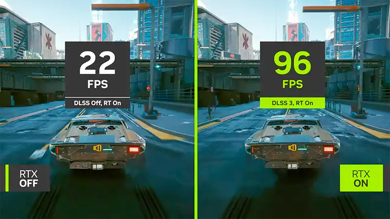
This new DLSS processes the new frame along with the previous frame to see how the scene is changing. The OFA provides the neural network with the speed and direction of the frame-by-frame pixels so that it generates completely new intermediate frames without having to process the graphics and involve the game. The performance can be up to four times higher than DLSS. DLSS 3.0 will work simultaneously with DLSS Super Resolution (DLSS 2), being an indispensable technique for demanding open-world games such as Cyberpunk 2077, A Plague Tale: Requiem or Flight Simulator.
The Nvidia RTX Remix add-on was previously shown before the release of Ada Lovelace, remastering the graphics of TES Morrowind and Portal. It is a ray tracing mechanism capable of transforming classic games by adding light and shadows through ray tracing using AI and DLSS. However, the quality or resolution of the textures remains the same, being the task of the modder in question to redesign these textures. The process uses a USD (Universal Scene Description) extractor that converts the game assets into an open 3D frame for the RTX Remix application to do its work. The NVIDIA RTX Path Tracing Software (SDK) development kit will be released for working with ray tracing and neural graphics for designers.
Final Words and conclusion about the Nvidia RTX 4090
We have before us the graphics card that will set the standard for the new generation, an impressive beast that has shown improvements of around 60% and even more compared to the RTX 3090 Ti in benchmarks and games in 4K and 8K resolution. Clearly, it is a GPU designed for rendering and work above UHD resolutions, as the results in 1080p and 2K are even modest due to the limitations of the CPU itself.
The brutal increase in processing units compared to the previous generation’s flagship leaves us with incredible rendering times thanks to the improvement in IPC and frequencies that border on 3.0 GHz on the 4 nm die. All of this while maintaining the same consumption as Ampere and good temperatures, although we pay the price with excessively large coolers.
All of this is added to the internal architecture improvements and updates of key technologies, such as the double AV1 encoder implemented in the GPU, which will allow streamers and creators to get much more performance in their work. DLSS 3.0 marks a new performance peak, even doubling in some cases the previous version thanks to the Optical Flow Accelerator and Nvidia Reflex, among other improvements.
Without a doubt, this Nvidia RTX 4090 gives us exactly what it promises, but its price, sitting at approximately $2,000 USD, it’s a cookie a bit harder to chew for some.
More stories like this
- NVIDIA GeForce GT 720 review
- NVIDIA GeForce GTX 1050 Ti Max-Q review
- NVIDIA Quadro FX 3800 review
- Nvidia Geforce GTX 560 Full Review
- All About the Ada Lovelace Architecture technology of the GeForce RTX 40 Series
- Nvidia RTX 3090 vs RTX 3090 Ti: The not-so-obvious conclusion