You can also be interested in these:
- What is Dark Silicon and what is it currently used for?
- Seemingly all Intel Alder Lake CPU can be overclocked after all
- Intel confirms Raptor Lake LGA 1700 and DDR4 compatible
- Comparison of the Z790 and Z690 Intel motherboard chipsets
One of the most crucial components for the semiconductor manufacturing industry is arguably the silicon wafers. A component that gives life to the hearts of all devices nowadays and also to other derivative products such as RAM memories. The technology of wafers have been advancing over the years, however they also have encountered many problems along the way. We are going to assess what is the reality in today’s semiconductor wafer manufacturing industry.
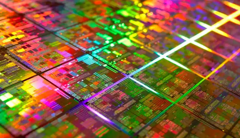
A wafer, also called a Slice or Substrate, is nothing more than a very thin layer of a semiconductor material, normally crystalline silicon. This component has a circular shape due to the semiconductor wafer manufacturing process and this where the chips will be engraved to give life to our products afterwards, CPU or GPU.
Its complexity lies in its purity, since the material must be a pure 99.9999999 (it is known as 9N) and will form with it the round sheets with a series of specific diameters and thicknesses after several passes in the processes.
The size and thickness of the wafer determine the number of operating chips
The sizes and thicknesses of semiconductor wafer varies, since each of the functions over the years has chosen its own manufacturing method. Therefore, defining these as standard measures is not only complicated, but in most cases they were exclusively used by a manufacturer, without it being globally produced.

Sizes refer to their diameter, which is the unit of measure of each type of wafer. This allows the size to increase as time progresses, making each wafer more and more profitable, since the larger the size it is possible to extract a greater number of operating chips from it.
The challenge has always been to create larger wafers while maintaining their quality and purity. In addition, the larger the size, the thickness has to be increased, which makes engraving the circuit pattern more difficult, but allows a greater number of layers at the same time.
The semiconductor wafer heritage
Types of semiconductor wafer
The first wafer was created in 1960, and as such, with low expectancies of its performance. By the time it was a milestone that marked the beginning of a new industry 70 years later. The first size was 23mm, although its total thickness is unknown, however it had to be somewhat low, like just a few micrometers.
In 1962 and after the semiconductor wafer manufacturing technique was refined, 25 mm wafers were achieved. The total thickness on these was not revealed, although it is believed that it would be about 130 micrometers approximately. Only one year later, in 1963, the 28 mm diameter was changed and with it the thickness increased again, (At that time it was difficult to have an accurate measurement of a component that small because they didn’t have the technology for it) but it is estimated that they would be between 180 and 190 micrometers.
The first chips and semiconductors had a solid introduction in the market and caused a revolution that never allowed the industry to stop growing. In 1969 the 51 mm wafers arrived, almost doubling the size in just 6 years. The thickness could be measured this time around (275 microns).
The semiconductor wafer manufacturing industry totally focused on improving wafers. In 1972 they came up with a 75mm diameter wafer, all this with an increased performance, thanks for the most part to the thickness of 375 micrometers. The industry saw great potential in wafers and the growth rate remained more or less stable, as 100mm and 525 micron wafers were launched in 1976.
It was another step forward that greatly profited the price of chips and fueled the wafer industry growth. In 1981 the size increased to 125mm and 625 microns, representing a growth of 25% per wafer in just 5 years.
The semiconductor wafer industry slowdown
Two years later in 1983 the industry reached 150 mm per wafer, setting the precedent for inches as the simplest measure to name wafers. The equivalence was 6 inches and was achieved thanks to a thickness of 675 microns.
The jump in size was 20%, but it was achieved in just two years. Starting in 1983, both Intel and the rest of the foundries found themselves with a difficult situation to solve. Since they required a new semiconductor wafer manufacturing process to create new units and continue increasing their size. in addition, the materials used needed a different processing in terms of impurities and of course, a greater thickness to be consistent.
It took 9 years until 1992 when the 200mm or 8-inch wafers were achieved. The thickness went from 675 microns to 725 microns. It again meant higher profitability and yield per wafer in the industry, but the slowdown was obvious and had no signs of improving.
It took ten years for the industry to make the next evolutionary leap in wafers manufacturing. At the moment in 2002 the current 300 mm or 12 inches was just being implemented, where once again the thickness increased to 775 micrometers. It represented a 50% jump in profitability and once again represented a boost of the industry.
The total cost was stratospheric, to the point no one has stablished clearly the exact number. The latter is believed to be around 20 figures, and is that exact type of semiconductor wafer we use nowadays.
A glimpse into the future of the semiconductor wafer manufacturing industry
We are at the beginning of 2021 and after long years of promises the industry cannot make larger wafers despite the huge amount of money that all foundries have invested. In this case, the figure is unknown, but many analysts say that the new 450mm wafers with 925 micrometers is a real money sink. For the industry it doesn’t have any sense to keep that route.
The industry is insatiable and with no view of a specific date to stop such investment. The launch date for these wafers will not be before 2025, since the process they are being subjected to requires a “culture” with materials added to the silicon to be able to handle the stress and deformation that is required in the cutting process.
It is rumored that the structural integrity of these wafers is the main problem they face, since although some manage to stay perfect after the original cutting, others suffer deformations during the processing or manipulation, thus rendering them useless.
The problem is reaching such a point that it is possible that we will reach the physical limit of nanometers earlier than the physical limit of wafers. It could be the case that the entire industry ends up allocating resources exclusively to creating larger diameters rather than reducing the size of the transistors.
Likewise, the recent addition of China into the semiconductors wafer manufacturing industry may be a turning point, not only because of the capital invested, but also because they currently own the fastest developing technology. The catch is, they first have to catch up and then finally innovate, so the 2025 date may fall a bit short if the problems continue and the sector does not have much more leeway, as Intel has stepped on the accelerator and will force TSMC and Samsung to do the same.
The prices in the wafer industry
It is one of the best kept secrets in the semiconductor industry, mainly because direct rivals struggle to offer the best prices for the most advanced nodes, and those that do not have them only have to play low. But they and their customers play a “give and take”, since the prices of the world’s largest wafer manufacturer, TSMC, have increase disproportionally.
We are always complaining about the price of AMD, Intel or NVIDIA components, but we rarely think about what all the components they include are worth. There are many of them that will not appear in at a retailer or wholesaler scope, not in the entire world. These are hidden or personalized prices for a certain production volume, which is why filtering this information today is so important.
How much has the wafer and chip value increased?
To understand the table above, you must first understand that the data are rigorous estimates, but they are not 100% accurate (market is quite sensitive to small changes). Additionally, the pricing model accounts for energy use, depreciation (important), chip assembly, testing and packaging costs, and of course foundry operating margins.
As for the chips, besides everything said, they come also with the cost of design, where the price is reportedly based on a hypothetical 5nm GPU, so we can have an idea of how the same chip influences the final price.
The duality on the price of wafers vs clips
From 90 nm to 16/12 nm the price scales more or less steadily, but from there we see how it doubles with each jump, where the 5 nm represents a more than considerable rise. In 16 years, the price has multiplied by 10.29, while the sale price of the chips has decreased in a very similar proportion: 10.22.
The problem facing the industry is that the cost to keep going down nanometers is going to skyrocket even more, which is going to mean a price jump per chip that could only be attenuated if larger wafers actually arrive to achieve more suitable chips per one of them.
On the other hand, the density of each of the nodes is not mentioned, something important that logically influences wafer prices, but to have a clear example, in the last three years and three nodes the density has multiplied by three , so the number of transistors is at least a similar factor, if not higher.
New scanners, new resistor processes and masks with EUV High-NA
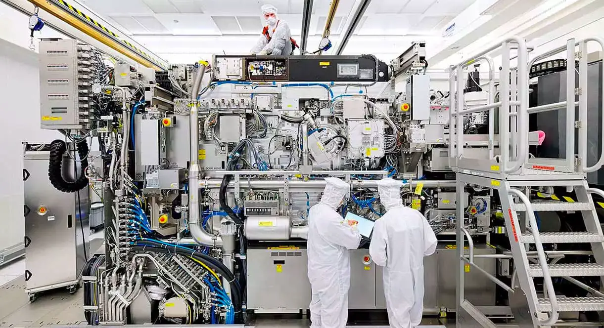
There are three main pillars of wafer engraving in today’s manufacturing industry and for years to come: the scanners provided by the aforementioned ASML, the resistors for the masks, and the masks themselves.
Why are scanners a problem? Mainly because reducing the wavelength of 193 nm is really complicated, since you need a 0.33 numerical aperture (NA) lens with resolutions of 13 nm and with the highest possible performance per wafer.
EUV is a technology that works with laser pulses that hit small droplets of tin at a very high speed, which generates photons and these bounce off various mirrors inside the scanner to end up reflected on the mask and then on the wafer, giving shape to the transistors.
The problem is not only that the photons do not end up on the wafer, or that they remain in the mask, the real problem lies if they are directly lost around the edges. The solution would be to use films that protect the wafer, but the technology is not readily available, so pushed by the competition, everyone has gone to engraving at 193 nm without them, which is feasible at 7 nm and the future 5 nm.
A simple and not multiple pattern is used, since it can have a pitch gate of 32 nm or 30 nm, but reducing it implies changing scanners to reach 3 nm or less. The answer will come back to ASML with a 0.55 NA scanner capable of recording at 8 nm resolutions, a gigantic advance.
These scanners will be called High-NA and will allow a return to the unique design pattern, reducing costs and progressively increasing wafers per hour. In order for them to work, two masks are required and not one, which have to be sewn together.
This will skyrocket the cost, which is already rather high today, since, for example, a current EUV scanner is over 153 million dollars, while the High-NA will be over 318 million. Does that mean that the processors will increase in price, as well as the GPUs? It is quite likely if they do not find a solution.
The resistors for wafers are also seeing a dead end
Before creating a pattern for a wafer, it is inserted into a system called a coater, in which photoresist materials are poured into the wafer, rotating to leave a uniform layer to protect it.
After that the engraving will arrive in the lithography scanner, so it is a very important preliminary process. Currently there are two systems to do this in EUV: chemically amplified or CAR and those based on the so-called metal oxide.
The problem with CARs is that they suffer from blurring on the scanner lens, therefore is not allowed such high resolutions in these. Not to mention those that come with NA. Metal oxide resistors are more suitable to bypass these failures, but on the other hand they are less stable, thus there is no system that is 100% reliable and above all profitable.
However, they are working on a system called “dry photoresist”, a system to remove moisture and improve resolution and stability by layering them in a dry processing chamber prior to exposure to photons. This will be valid for EUV and EUV NA, but it will take a few years to arrive.
Finally the photomasks
A current EUV mask consists of between 40 and 50 thin layers of silicon and molybdenum on a substrate, giving a total thickness that is usually between 250 nm and 350 nm. Each mask has a component called “absorber” which prevents light bouncing off the wafer and helps a more perfect etching.
The challenge with these is that in an EUV system the light reaches the mask at an angle of 6º, which enhances the fact that it is reflected and the absorbent cannot do all the work, causing possible changes of location in the patterns, with the consequent deterioration of the wafer.
How to solve this? With finer absorbents. The current ones are 60nm and the best and most expensive 50nm, but they are not able to fix this and less at smaller and higher wavelengths. For this reason, the researchers are creating two new types of masks for future lithographic processes in EUV: the so-called High-K and the Phase-Shift.
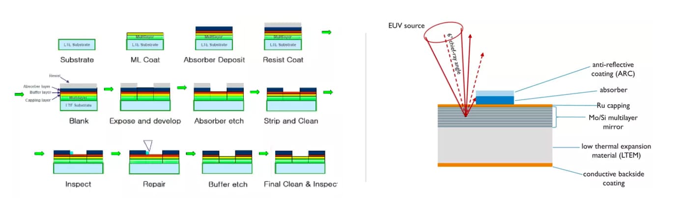
The latter are the simplest, because it only requires changing the absorbent material for one with Low-N properties, leaving aside the tantalum. What is sought is to block the light and prevent it from being reflected, achieving dark areas and therefore improving the precision of the images with more basic contrast.
Very little is known about High-K, but it seems that they can be repaired with a laser, lowering the final manufacturing costs, since the masks are extremely expensive and one is needed for each pattern.
In summary, the 7 nm and 5 nm are guaranteed, but going down to 3 nm is not going to be so easy despite the fact that both Samsung and TSMC and Intel claim to have them ready by 2025 in the worst case scenario.
More stories like this
- What is Dark Silicon and what is it currently used for?
- Seemingly all Intel Alder Lake CPU can be overclocked after all
- Intel confirms Raptor Lake LGA 1700 and DDR4 compatible
- Comparison of the Z790 and Z690 Intel motherboard chipsets
- Who leads the battle of the CPUs in 2023?
- AMD Ryzen 7000X3D: What to expect from these new CPUs?