You can also be interested in these:
- What to look out in a cheap high-quality camera
- How to diagnose errors on your webcam
- How to fix the Wyze error code 90
- Is your Lenovo camera not working? Learn how to fix it
The phone cameras from 10 years ago, where there were at its most 2 MP resolutions, are nothing like the ones we have nowadays. The advancements on this field permitted a great deal of improvement in functionality and capabilities. Today, is quite common to see phone cameras with 5 lenses and sensors with as much as 108 MP resolution, like the newest Samsung Galaxy S21 Ultra. While the cameras and resolution have increased significantly in the last couple of years, the lens technology we have today is the same since its origins.

Almost out of nowhere, a new company called Metalenz disclosed an interesting concept that might revolutionize the phone camera manufacturing industry. The company introduced the optical metasurfaces technology, which offers new and more optimal methods of light collection and sensing for better quality images. All this, without taking too much space and processing.
How do camera lenses work?
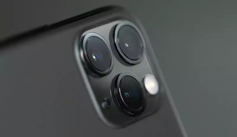
Phone with many cameras also have, for each individual unit, a stack of up to 7 lenses on top of each other. This is where technologies like the Carl Zeiss optics come into play. If you were to have only one lens on a camera, it would be a lot more prone to show irregularities, like chromatic aberrations or lens distortion. Adding more lenses for every single camera allows phone manufacturers to compensate these irregularities. Although, this comes with a price: the more lenses you stack the more bulky your camera will be.

Phone companies have fought this problem since forever, creating technologies to counteract this effect. Companies like Samsung created “periscope” lenses to have the effect of a regular one in a more compact space. Despite this effort is indeed one step in the right direction, we are still using the same technology for this purposes.
Metalenz is ready to takeover the camera lens industry
Up until now, no company have taken a step back and visited the drawing board once again to assess a new way of making this work. The new Metalenz technology uses a single lens in an array-type nanostructure, sandwiched in between a thin layer of glass. Those nano sensors bend light successively to correct many of the problems conventional lens systems do.
This new technology, with over a decade of research, reinvented the way phone cameras work as we know them. The nanostructure present on the Metalenz, when seen through a microscope, shows an intricate pattern of circles of different diameters. The function behind those is to speed up and slow down the light as it passes through them. This process allows the lens to reconfigure and correct the image, according to Robert Devlin, co-founder and CEO of Metalenz.

The resulting image with this technology is many times sharper and brighter than the conventional methods. The way the Metalenz handles the light permits the technology to require a lot less and deliver incredible results. It not only produces higher quality images, it does so in a more streamlined and optimal process with just one lens.
Above all this, the company recently partnered with 2 major semiconductor manufacturers and has an incredible production potential. According to Metalenz, they are able to produce literally “Millions” of chips a day. This will ensure the company to satisfy the demand of the product and leverage the possibility to build units in the same facility that creates devices potentially needing this technology.
How Metalenz does things differently?
The technology present in mobile devices is not very forgiving on the unit’s resources, specially power consumption. Current 3D sensors, like the Apple’s FaceID recognition system shoots lasers to brighten the scene and capture the image data. By using the Metalenz, the company assures the same result can be achieved maintaining the quality and having a considerable less amount of power expense.
Another advantage among the major benefits of using this technology is the space. By reducing the foot print of the lenses, the amount of space reduced can bring a new meaning on the placement and distribution of the modules and functional elements of the phone. No more bulky cameras sticking out from the glass or device cover. The new cameras under this technology can be so thin, they would fit comfortably under the glass of the screen, inside the unit.
The spectrometer for instance, is used normally to sense the light wave length and identify different molecules in the blood, in health applications. The optical metasurfaces technology allow such compression in the components layout that can be possible a similar arrangement in a device as small as a smartphone. The uses and applications are countless.
When will we be able to see this new technology?
This is definitively the future of the mobile camera lenses. However, this technology can be extended to any other application which requires camera lenses, like virtual reality gaming, car rear cameras, devices in the health industry, etc. The range of uses and applications is almost endless.
The company is planning to mass produce the Metalenz by the end of the year. The first appearance of this technology will be on a 3D sensor lens in a smartphone, although we don’t know which one yet.
More stories like this
- What to look out in a cheap high-quality camera
- How to diagnose errors on your webcam
- How to fix the Wyze error code 90
- Is your Lenovo camera not working? Learn how to fix it
- AMD Zen 3 vs Zen 4: The evolution and revolution
- What is the AMD FidelityFX Super Resolution?